Hi @omap7 and welcome.
One is for 44100 Hz sampling rate and other for 44800 Hz.
With just one crystal and if you plan to use alternatively one and the other sampling rate, it will work nicely if it fits the right crystal clock otherwise some compute overhead will be needed to resample the data.
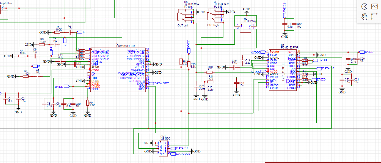
I have try designing a PCM5122+1863 soundcard ago,but I haven’t use any crystal and two chip’s SCK were pulled down by resistors .It works correctly all the time .TI’s manual says the crystal is not necessary ,If I delete crystal ,will it generater some harmful effect? I’m not very sure.
Ok, firstly I had a look at my IQaudio DAC Pro wich runs a pcm5242: they are no clocks on board.
from pcm 5242 datasheet page 47
The device has an internal PLL that is used to take either SCK or BCK and create
the higher rate clocks required by the miniDSP and the DAC clock.
When just using BCK, the chip will be in “Clock Slave Mode with BCK PLL to Generate Internal Clock” see 8.3.3. The quoted is then folowed by:
In situations where the highest audio performance is required, it’s suggested that the SCK is brought to the
device, along with BCK and LRCK. The device should be configured so that the PLL is only providing a clock
source to the miniDSP. By ensuring that the DACCK (DAC Clock) is being driven by the external SCK source,
jitter evident in the PLL (in all PLL’s) is kept out of the DAC, Charge Pump and Oversampling system.
So using external clock is highly recommended.
While it looks like pcm51x and pcm54x series when configured in hardware mode can automagicaly adapt their pll clock (from 8.3.3):
In hardwired mode, the device starts up expecting an external SCK input, but if BCK and LRCK start correctly
while SCK remains at ground level for 16 successive LRCK periods, then the internal PLL starts, automatically
generating an internal SCK from the BCK reference
when using I2C mode, some registers have to be set:
#******************************************************************************
#  PCM512x,4x,5x Code Example: 3pin I2S input (no master clock)
#
#  Description: The PCM51xx family in software mode (I2C or SPI) require the Clock Tree and PLL
#	to be configured based on knowledge of the incoming Bit clock (BCK) reference. The code below assumes
#  a 64fs BCK on 48kHz data. The PLL needs to be configured to create a faster clock rate for the miniDSP.
#	(the miniDSP typically runs at ~50MHz).
#
#	#### CLK divider setting ###################
#  #### Use VREF PLL settings when in VREF mode to look up the sample rate, and the SCK ##
#  #### The table assumes SCK as a reference - but the same frequency can be used with a BCK reference##
#  #### In this example, look for 48kHz rate, with 3.072MHz SCK ####
#
#	Connection
#
#	SCK : do not connect
#	BCK : input terminal
#	LRCK : input terminal
#	DATA : input terminal
#
# 	Commands below are written in the TI-Tools for for I2C. (Codec Control, Purepath Console and Purepath Studio all support this format).
# 	Format:
# 	A BBh CCh DDh
#
# 	A = R or W (read or write)
# 	BBh = I2C Address (98 in this case)
# 	CCh = Register
# 	DDh = for Writes, it's the data, for reads, it's the number of bytes to read back.
# 	Either # or # can be used for comments.
#
#  Dafydd Roche
#  Texas Instruments, Inc
#  August 2013
#******************************************************************************


# Auto divider setting : disable auto config and ignore SCK losses
w 98 25 1A
# PLL P divider to 3
w 98 14 01
# PLL J divider to 16.D1D2
w 98 15 10
# PLL D1 divider to J.00
w 98 16 00
# PLL D2 divider to J.00
w 98 17 00
# PLL R divider to 2
w 98 18 01
# miniDSP CLK divider (NMAC) to 2
w 98 1B 01
# DAC CLK divider to 16
w 98 1C 0F
# NCP CLK divider to 4
w 98 1D 03
# OSC CLK divider is set to one (as its based on the output from the DAC CLK, which is already PLL/16)
w 98 1E 00
# FS setting should be set to single rate speed (48kHZ).
w 98 22 00
# IDAC1  sets the number of miniDSP instructions per clock. (set to 1024)
w 98 23 04
# IDAC2
w 98 24 00
#############################################


# Set PLL Clock Source to be BCK instead of SCK
w 98 0D 10


#### Stand-by request and release ############
# Stand-by request
w 98 02 10
# Stand-by release
w 98 02 00
##############################################
was the example for a “no crystal” setup taken from https://e2e.ti.com/cfs-file/__key/communityserver-discussions-components-files/6/SLACC622.zip
(include also examples for master and slave setup with an external clock)
In our case this configuration is done via software
- on the audio board driver level
Example: here for the hifiberry dac plus:
- and on the audio codec level itself
(pcm5122 for hifiberry dac plus):
Finally TI’s typical application of pcm5242 is a “High Fidelity Smartphone Application” wich doesn’t show any crystal (figure 80 page 60) and I’m really happy too with my IQAudio DAC without crystals, so I understand your questioning: why the hassle ?
We use high preccission oscillators (20ppm) for ultra-low jitter sampling and it cost about 1€/piece. Do you want to resample audio data for saving 1 €.? Not in my town …
of course not ![]()
Clock jitter adds noise (pink noise?) in the conversion process, so lower the jitter, better the result. Of course, jitter it’s not the only factor to keep in mind, but it’s a factor quite easy to improve.
If you don’t include dedicated clocks, the DAC/ADC will use the RBPi’s internal audio clock and your DAC/ADC chips will be synced to it . RBPi’s clock has a given precission and the jitter will be according to it. Also, RBPi’s clock is “far” from DAC/ADC chips, what it’s not good for stability.
If you add external clocks, your DAC/ADC chips will be synced to them instead of RBPI’s clock. If your external clocks are good enough and you place them very close to the DAC/ADC chips, you will get a lower jitter & improved stability so your audio will be better. I mean, the DAC’s digital input will be more accurately converted to an analog output signal and the ADC’s analog input signal will be more accurately converted to a digital stream.
Oscillators are cheap (including good ones with precision of 20 ppm or less) and you can copy the ZynADAC design, so i can’t see any reason for not doing it. Up to you!
Enjoy!
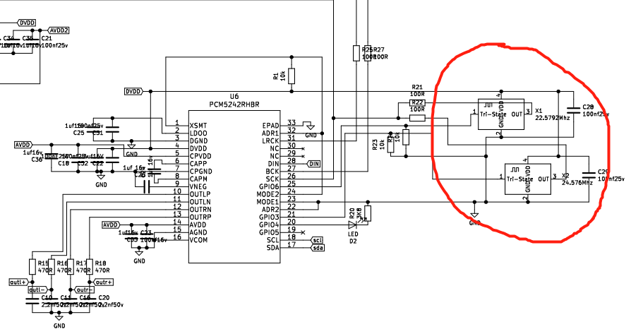
Yes , when I see the ZYNdac first time , I was shocked by these two crystals! It is the first time I know that you can parallel connect two different crystals to obtain multi-frequency support.(I think it’s a nice and creativity design).So,I do a lot of test for the feature about PCM5122&5242,I found that if you disconnect crystals ,it still works.As you said ,it’s better to use crystal to decrease jitter.  But I always afraid some frequcney problem will occur
  , I rememberd that the superposition two different frequency sin wave will generate some other frequency , it a mathmatical problem , should I think it about?
Oh!Thank you for your detailed analysis.  I decide to redesign my PCB,add two crystals to decrcase jitter (as ZYNdac),some Xrun occured before , I don’t know whether this problem lead by these two crystals.