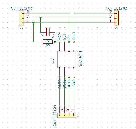
I did construct that fritzing sketch using that picture. It is not same?  How I should change it other than remove DATA line resistors?
Electrically is the same.
But in the final design (I mean, I don’t think you’ll build a synthesizer with a breadboard inside  ) you don’t have to bring all 5Vs and all GNDs to the same points, like you did in the sketch.
Oh yes. Now I undestand 
I did contact designer of that 5v 3.5a UPS board and he said that there will be no more boards for sale. 
I must order my own PCB from OSH Park. I get 3 PCBs for $26.35 and there is free shipping.
1 Like
Hi @Aleksi!
I see you are using Fritzing. I was using it too some time ago, but when schematics start to grow in complexity (and yours is quite complex right now  ) you will realize that Fritzing is not a “serious” tool and you will waste your time fighting with the software. The Fritzing’s schematic tool is very poor, and the PCB designer is not much better. When you have to add some new component to the library, you will see that the footprint designer is almost useless and you need to use inkscape and edit coordinates by hand … a nightmare!!
Why not using Kicad? I did the change in a few days and believe me, it’s the best time investment you can do.
Perhaps this post can help you to change:
Kind Regards,
3 Likes
Lol. Thanks for that post. I will read it carefully.
Edit.
I found out that I had Kicad already installed. I did install it 1 year ago.
I did my first schematic in Kicad. (I followed tutorial at hackaday. Nothing related to this project) I will finish it today and start working on PCB for WS2811 and HC4067 chips if it does not take too long.
I realy like that you can see your board ready in the end and all those hotkeys.
Edit.
It did not take long at all. I did finish it some time ago and will start making schematics for synth PCB.
1 Like
I realy like […] all those hotkeys.
Great! ![]()
BTW: All those hotkeys are why most peolpe hate KiCad!
People that never user a PCB CAD before, obvoiusly. I started making PCBs many years ago with MS-DOS tools and they were all hotkey-based. When one gets used to use hot-keys, he realizes how much faster is he working…
1 Like
1993 i made my first pcb
the type of pcb that you manually apply the traces and pads to etc
we didn’t have computer software at the time, it was a gruelling job
we got the job done, not made many since then though. might have to start looking into making something again, whats the best freeware type of program there is for pcb design
@christianforshaw in 1993 I was already using photo-resist and photographic masters plotted (with an original Roland 7475) on transparent sheets…
I made my first PCBs in '85 using those “rub down” transfer sheets with pads and traces, and the mighty “EDDING 3000” felt tip pen to fix mistakes. It was a pain in the ass! I started learning the photo resist process, built my own two-side UV bromograph, and never made another PCB by hand.
I was 13. 
brings back memorys that @Axeman … 93 was my first year at electronics school , 16 at the time, a small part of it was pcd design and prototype
made a analogue to digital convertor sample pack for my amiga 500 , hacked a original sampler up and made a few runs of it, kind of a chineese sweat shop,but in uk haha
Wow. You guys have been doing this for long time. What is your favorite project that you have done?
At this moment I am trying to design breakout board for WS2811 chips. I will use 3 connectors per board. First for input singal, GND and input voltage. Second for output singal, GND and output voltage. Third for led wires.
Well it did not take long to finish schematic. Does this make any sense to you?
Should I use GND label or GND component at ground pins and connectors?
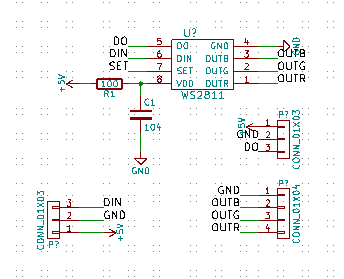
IMHO you shouldn’t use named nets and signals just for a pair of connection. It renders small schematics difficult to read…
I did not think about that. Thank you. I will change it.
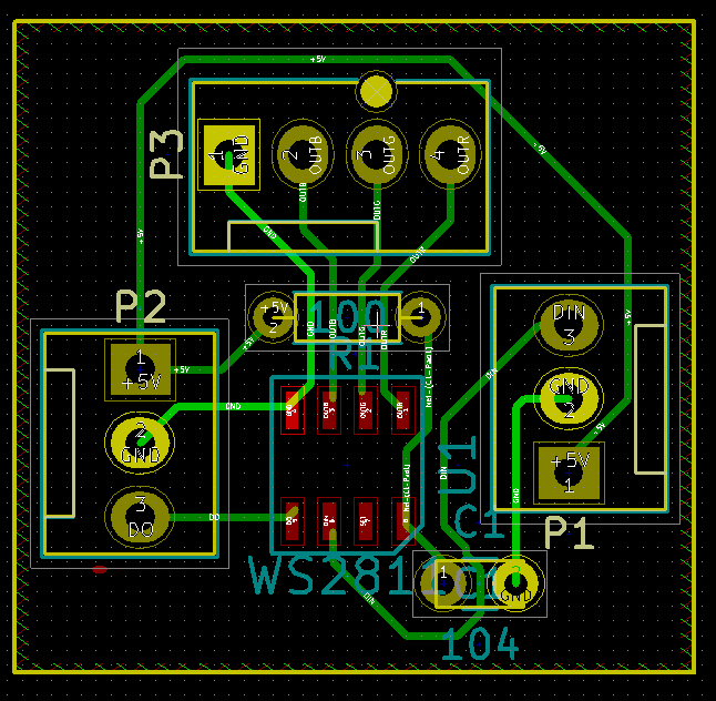
Here it is. I managed to make it one sided but I think that I made copper lines on wrong side.  Is there easy way to fix this?
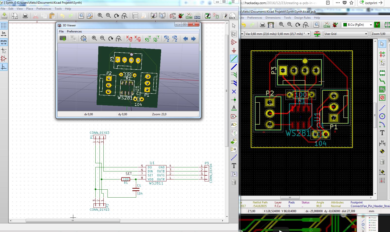
(Edit. If you look closely you can see that there is one mistake in schematics. VDD is connected to DO.)
What ways have you used to make PCBs? I think that I want to make all 22 boards by my self.
Edit.
Well I fixed it. I hope there was something to be fixed.
This was so fun that I think that I wll start designing PCB for other chip right away. Or after I have eaten somethig.
There is no “right” or “wrong” side. You’ve chosen a SMD package for WS2811, so tracks must be on the same side as the component.
Do a “real world” test, and print it on paper
Oh no. I must fix it then. How then can I mount the through hole components to board if copper is on top? Do I have to make board 2 sided?
“You’re non thinking fourth-dimensionally, Marty” 
If you have to go single sided, then all tracks and SMD components go on the bottom side, whereas THD components, connectors, etc. go on top side.
rofl:smiley: Ok. Thank you so much for help. You are the best.
Edit.
Now it is fixed. Tracks and SMD components are on same side.
