i also used sockets for ICs, in case i need them again ![]()
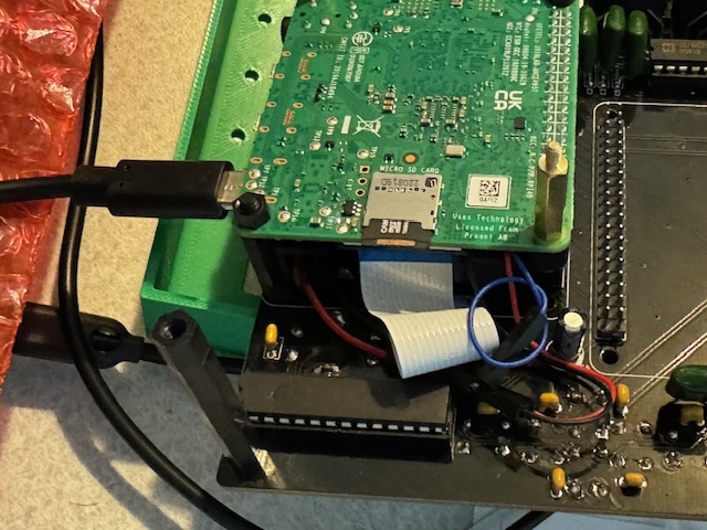
i also used sockets for ICs, in case i need them again ![]()
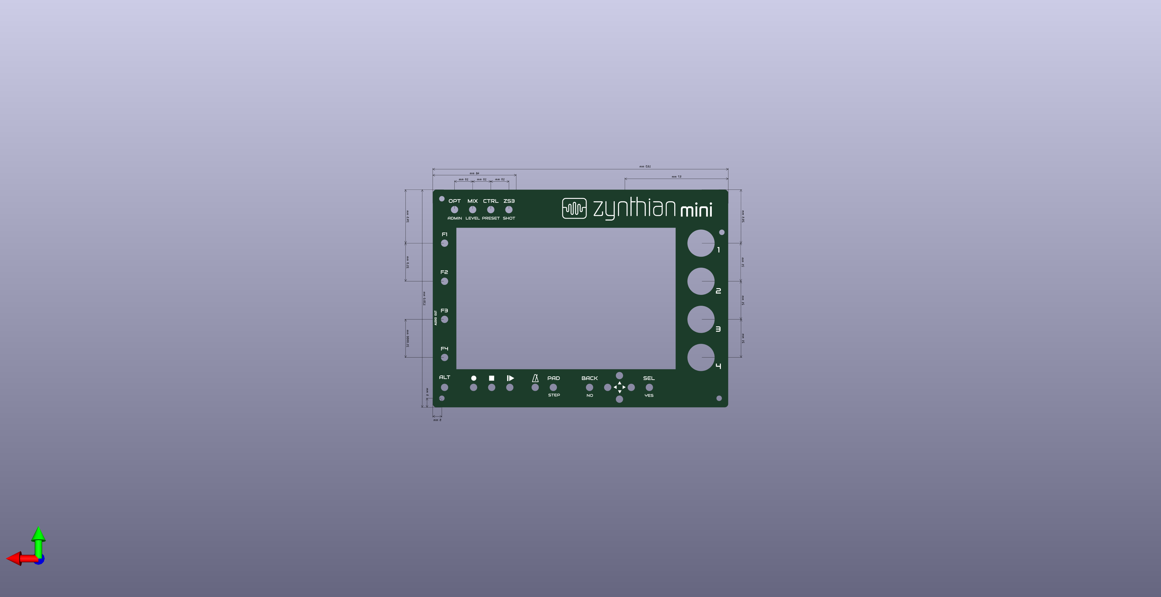
It looks better that the buttons are arranged at on line.
Could someone tell me which files are needed for a service like jlcpcb.com?
Thanks
@JayBee - you will need to open pcb in KiCAD 8.0 and plot gerber files.
I will order another batch of 5 pcbs with pcbway that will include a small change for bottom section buttons aligment so that their labels can fit better. Expect that in couple of days. I will share a link of my order so that everyone can just click on it and order the same.
agreed
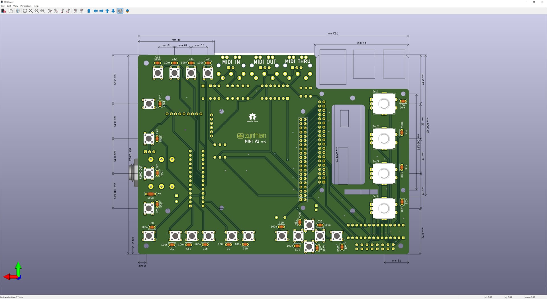
Almost finished with in line bottom buttons design.
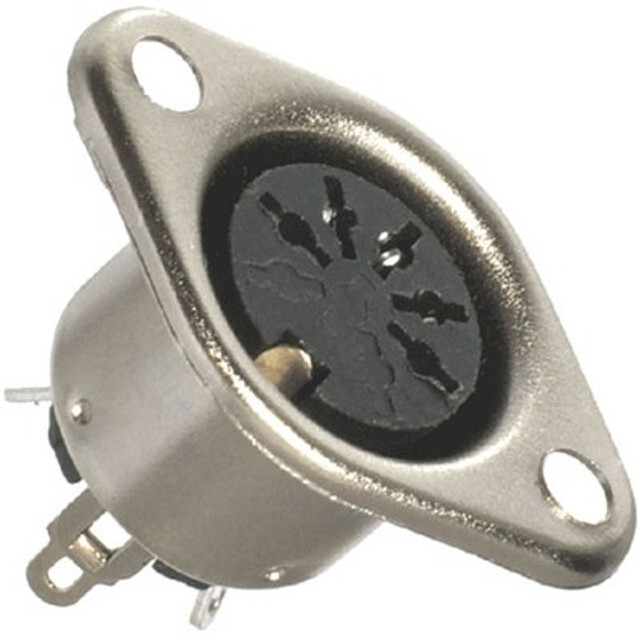
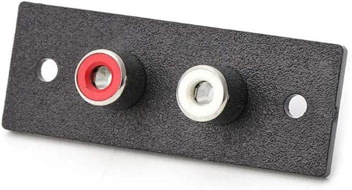
Also I have added additional connectors for all MIDI and AUDIO-OUT connections so that this can be incorporate into the case which edge does not come to the edge of the PCB and where PCB mounted connectors are not appropriate and where panel connectors like this need to be used :
and this
I have remove PCB mounted RCA connector from design. My RCA footprint did not work and instead of fixing it I decided to remove it from design because these PCB mountable RCA connectors comes with many different footprint shapes and any RCA panel connector can be used instead by connecting to now available connector. I have left PCB mountable 1/4 stereo jack only for audio out.
@nanomole I like the i2c audio card sockets that you used. Having them you can easily remove the card and put some other into the HAT . I am not sure that you will ever be able to run both at the same time. Most of cards use the same rpi pins for data line. Hence a different microchip DAC will need a different driver that can not support both at the same time.
Such great work in such a short time. Is there a bill of materials somewhere? Including optional items like compatible sound DAC’s.
The one suggestion I would make. Perhaps add button function labels (or icon) on the PCB adjacent to the buttons (if it is possible to fit) or a button function diagram nearby that will be visible when assembled. I can see myself doing a barebones one of these with out a case and knowing what the buttons are will likely help me.
@pac_71 - I am working on front facia that can be produced as PCB insetad of laser cutting acrylic and engraving. Almost there:
Just to add few labels for connectors.
@pac_71 - bill of materials is on zynthian mini wiki
As you are redesigning the pcb. Can you take a look about the dsi cable and the raspi 5?
Imcan take a look on my raspi5 tommorow.
Good point - I will check this.
The mini design might allow for more franken-Zynths with other similar RPi modules like Rock Pi 4/5, Risc-V SBC, etc. Obviously YMMV with building the right Zynthian OS.
Simple question for guys that are better in electronics than me. I have 4 microchips on the MINI V2. They all have 100n filter capacitor on their 5+ power lines connected to ground which is a common practice to remove noise from the power . That means that I have 4x100n capacitor in parallel between 5+ and ground.
Is this unnecessary - should there be only one ? are they still working as a proper filter because 4 capacitors in parallel are now producing 400n capacitance instead of 100n ?
I have not spotted any issue while testing this config but if this is not right I would like to know.
I would not say that I’m better because I’m discovering practical electronic only since I discovered Zynthian.
But so far I’ve seen:
It’s common practice and normally recommended in most datasheets to place decoupling capacitors on every chip, as closed as possible to the physical power pins. “As closed as possible”, this is a key detail. Decoupling capacitors are not only about “power noise”, they act as “power buffers”, that can supply very quickly the current peaks demanded by ICs, reducing current peaks along the PCB power tracks and reducing power voltage fluctuations due to track impedance.
Cheers
Your “simple question” is a surprisingly complex question and answer.
The “rule of thumb” I use is:
~100 nF ceramic per logic IC (multiple ones for complex ICs), combined with electrolytic or tantalum capacitor(s) up to a few hundred μF per board or board section.
That came from the Wikipedia article on “Decoupling capacitor” aka “Bypass capacitor” which you can read if you’re interested:
And, if you’re really interested you can take a look at the references in the article, they are excellent.
TTL - the logic family for ICs before CMOS needed much more bypassing. In general it is fine to have more bypass caps than you need. Ground planes can reduce the need for bypass caps. But you should have 1 big one (at least) for the incoming power and liberally sprinkle them around the board to give every chip the power it needs when it needs it.
Thanks all for great answers in regards of caps. I thought about moving few caps further away from their mc purely for aesthetic reason. I will not do that.
Indeed, the purpose of those decoupling capacitors is to provide filtering close to the chips. Moving them further away or combining them removes their reason for being there. It relates to high frequency oscilations that can occur over long (more than a few millimeters) PCB tracks. The capacitor sinks these hf currents before they have a chance to build. If you want an analogy, you can think of there being small pools of water that can slosh about and build into larger waves and the capacitors act as holes in the river bed that allow the water to flow away before they cause such waves. Of course this is just a daft analogy that doesn’t really stack up when using real science (you could say it, “doesn’t hold water” - an English colloquialism!) but it might help visualise why it is important to have decoupling capacitors at strategic physical locations.